Bachelor and Master Projects
We are looking for motivated BSc and MSc students to join our group for their research projects.
Do you want to do your research project in our group? Do not hesitate to contact us to hear about open projects!
Open Research Projects (more available! contact us):
------------------------------------------------------------------------------------------
Optoelectronic and Topological Phases in Moiré Systems
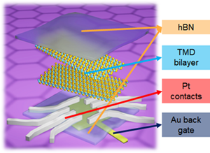
Two-dimensional (2D) Transition Metal Dichalcogenides (TMDs) are materials composed by a transition metal atom (M) sandwiched between two layers of chalcogen atoms (X2). A combination of different elements (for example M = Mo, Nb, W, Zr and X = S, Se, Te) can lead to a wide variety of optical and electric properties, ranging from insulating, semiconducting and semi-metallic behaviour. Furthermore, as the electronic structure depends on the thickness, the band gap evolves from an indirect to a direct nature as the thickness is reduced to a single layer.
Besides these material’s natural symmetry, a further superlattice symmetry within these systems can be achieved by stacking two of them with a relative twist angle (θt=0° only for different materials).
In these systems, local electric fields can be used to dope the Moiré and access several electronic phases including a Quantum Anomalous Hall (QAH) phase. This phase is characterized by quantized conductance and the presence of edge channels.
In this project, you will use high-quality crystals provided by the world-leading company in the growth of 2D materials - HQ Graphene - and use the cutting-edge nanofabrication tools present at the Nanolab Zernike to fabricate field-effect transistors based on Moiré heterostructures. Using the experimental setups and know-how already present at the Optospintronic of Nanostructures group, you will then perform the electronic and optoelectronic characterization of your devices at cryogenic temperatures and external magnetic fields.
Contact for more information:
Cedric Cordero (PhD) – c.a.cordero.silis rug.nl
Marcos Guimaraes (Assoc. Professor) – m.h.guimaraes rug.nl
------------------------------------------------------------------------------------------
Micromagnetic simulations of electrostatically formed magnonic crystals in 2D materials
As in an optical fiber, light can be guided by periodic modulation of the index of refraction using an alternating stack of two different materials, creating a one-dimensional photonic crystal. These photonic crystals have a photonic band structure, like their electronic counterparts where atoms are placed in a periodic grid giving rise to a band structure for electrons. Photonic crystals have broad application including optical filters and reflectors, lasers and quantum computing.
Analogous to how photonic crystals control light, magnonic crystals can be used to manipulate spin waves (magnons) – elementary excitations in magnetic materials. Magnonic crystals have periodic variations in their magnetic properties creating band gaps which can be used for spin-wave control.
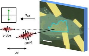
Recently, the OptoSpintronics of Quantum Materials group have optically excited spin-waves in a two-dimensional magnet [1] (Figure 1) – layered magnetic materials, only discovered in 2017 – and controlled its propagation using electrostatic gating. The goal of this project is to build on this work via micromagnetic simulations of 2D magnonic crystals created using finger electrostatic gates. This project will initiate a new research direction in the OptoSpintronics of Quantum Materials group towards electrostatically formed magnonic crystals.
References :
[1] Electric control of optically-induced magnetization dynamics in a van der Waals ferromagnetic semiconductor. F. Hendriks, R. R. Rojas-Lopez, B. Koopmans, M. H.D. Guimarães. Nature Communications 15 (2024) .
Contact for more information:
Samer Kurdi (Postdoc) – s.kurdi rug.nl
Marcos Guimaraes (Assoc. Professor) – m.h.guimaraes rug.nl
------------------------------------------------------------------------------------------
Fabrication of exciton insulators using TMD heterostructures
In the field of condensed matter physics, the quest to understand novel quantum phenomena has been a driving force behind groundbreaking discoveries and technological advances. Among these phenomena, exciton insulators stand out as intriguing quantum states with profound implications for both fundamental physics and practical applications.
Excitons are quasiparticles formed by a bound state between an electron in the conduction band and a hole in the valence band. If we can get all the free electrons in the conduction band to bind to the corresponding holes in the valence band, we will have no electrons to conduct.
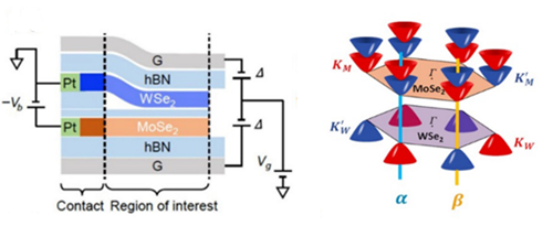
This project will consist of creating a heterostructure of graphene as the bottom and top gate, and a hetero-bilayer of WSe2 and MoSe2 encapsulated between two hBN flakes. By adjusting the bias applied to the two electrically isolated monolayers to a range where the injection of electrons and holes is balanced, and thus the carrier injection occurs in the form of bound excitons, there are no extra free electrons or holes in the system. In this situation the heterostructure becomes exciton-compressible (excitons can be injected into the system) but charge-incompressible (charge cannot be injected into the system and it is therefore an insulator).
References :
Tang, J., Zheng, Y., Jiang, K., You, Q., Yin, Z., Xie, Z., Li, H., Han, C., Zhang, X., & Shi, Y. (2023). Interlayer exciton dynamics of transition metal dichalcogenide heterostructures under electric fields. Nano Research.
Contact for more information:
Teresa Lopez (PhD) – m.t.lopez.carrasco rug.nl
Marcos Guimaraes (Assoc. Professor) – m.h.guimaraes rug.nl
------------------------------------------------------------------------------------------
Calculations of spin-wave spectra in novel 2D magnets
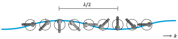
Spin waves are wave-like excitations in magnetic materials. They have nanometer wavelengths, gigahertz frequencies, and can even exist in insulators where they are free of the heating produced by electric currents. This makes spin waves promising candidate signal carriers for future information technologies [1] (Figure 1)
The OptoSpintronics of Quantum Materials group have recently probed spin-waves in a two-dimensional (2D) magnet [1]. Spin waves in 2D magnets offer an exciting route towards energy efficient and nanoscale computation devices. However, their spin wave spectra occur at challengingly large GHz to THz frequencies due to large magnetic anisotropies. The development of novel 2D magnetic materials is therefore increasingly more urgent.
Recently, a new group of 2D magnets have been synthesized based on the intercalation of the widely studied antiferromagnetic 2D magnet, MnPS3. The degree of intercalation is achieved via a molecular cation (tetramethylammonium) in which has significant effects on the magnetic coupling of MnPS3, converting it from an antiferromagnet to a ferrimagnet, offering a down conversion of spin-wave frequencies from THz to the GHz regime.
The goal of this project is to analytically calculate the spin-wave dispersion of intercalated MnPS3 via deriving the spin-wave equation of motion, using the Landau-Lifshitz-Gilbert equation, which governs the precessional motion of magnetization in the presence of effective magnetic fields. This work offers a promising route towards spin-wave resonance experiments and for realizing spin waves in 2D magnets at promising GHz- frequencies.
Reference:
[1] Electric control of optically-induced magnetization dynamics in a van der Waals ferromagnetic semiconductor. F. Hendriks, R. R. Rojas-Lopez, B. Koopmans, M. H.D. Guimarães. Nature Communications 15 (2024).
Contact for more information:
Samer Kurdi (Postdoc) – s.kurdi rug.nl
Marcos Guimaraes (Associate Professor) – m.h.guimaraes rug.nl