New Technique Unlocks Scalable Production of Next-Generation Electronics Materials
A team of researchers around Dr. Antonija Grubisic-Cabo has pushed the high-quality production of advanced materials that could power the next wave of electronics and computing. These materials, called two-dimensional (2D) transition metal dichalcogenides (TMDCs), are ultra-thin sheets just a few atoms thick and have the potential to outperform today’s semiconductor technologies. But until now, making large, high-quality samples has been a significant hurdle.
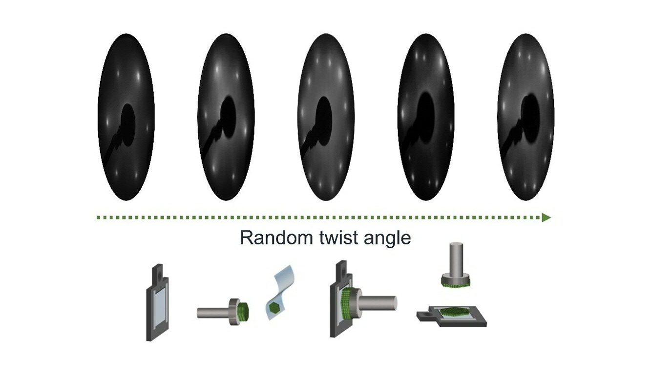
In a new study, Z. Dan and colleagues (2025) successfully created large, high-quality TMDC films using a novel technique called KISS — short for Kinetic In Situ Single-layer Synthesis. This method produces films up to 750 micrometers wide (about the width of 10 human hairs) under ultra-clean vacuum conditions, avoiding the contamination problems common in older methods.
Unlike traditional techniques, which often produce small and flawed flakes, the KISS method creates smooth, uniform sheets by taking advantage of strong attraction between the material and its underlying metal surface, all while keeping the environment perfectly clean. This allows for larger and purer films that are ideal for building new electronic devices or running high-precision experiments.
Careful testing confirmed the excellent quality of the new films. They were smooth, evenly spread in a single layer, and free from unwanted chemical bonds. The underlying metal surfaces also stayed intact throughout the process. Interestingly, one material, WSe₂, proved even easier to produce than others — likely due to its unique chemical properties.
This advance opens the door to making large, ultra-thin materials more reliably and at scale — a key step toward developing faster, smaller, and more powerful electronic and photonic devices. The technique also promises to accelerate research in nanotechnology and surface science.
Petra Rudolf and Antonija Grubišić-Čabo, Front. Nanotechnol., 02 May 2025
Contact: Dr. Antonija Grubišić-Čabo
More news
-
-
15 September 2025
Successful visit to the UG by Rector of Institut Teknologi Bandung
-