Towards all-electrical two-dimensional spintronic applications
The van Wees group has fabricated nanodevices that enrich the excellent charge and spin transport properties of graphene by bringing it in contact with other two-dimensional materials. They showed that in these van der Waals heterostructures a pure charge current creates spin currents, which makes them promising candidates for the future of spin-logic devices. The team was able to actively generate and manipulate the spins in the graphene only by electrical means without the need for magnetic fields or magnetic elements in the electronic circuits. This experimental observation is an important step towards all-electrical two-dimensional spintronic applications.
“Spin” is a quantum property of an electron that is viewed in a simplified classical picture as rotation of the electron around its own axis. Depending on whether the rotation happens in clockwise or anti-clockwise directions, the spin can be either up or down. The two well-defined states of the spin can potentially be used to store and/or transfer information (spin up = logical one, spin down = logical zero).
Generation/manipulation of electrons’ spins is the goal of spintronic devices in order to create and transfer the information faster with lower power consumption. Graphene has shown over decades to be an excellent material for transfer of electrons and their spins over long distances (tens of micrometers). However when it comes to active creation and control of the spins, graphene fails. That is because graphene does not have the intrinsic means to influence the spins of electrons, which requires “Spin-orbit interaction (SOI)”.
SOI, describes the interaction between spin of an electron and the direction of the electron’s motion. This means when we move electrons (charge current) in a material with strong SOI, the spins of the electrons get polarized (up or down) and as a result we can have accumulation of spins and/or generation of spin currents, due to the so-called charge-to-spin conversion mechanism.
The SOI is weak in graphene because it is made of light carbon atoms. However, in the library of two-dimensional materials, we can find transition-metal dichalcogenides (TMDs) that consist of heavy elements such as tungsten and sulfur (like WS2). Just like graphite, WS2 has layered crystal structure, monolayers of which is readily accessible by peeling off the bulk crystal by sticky tapes. If we bring the single layers of WS2 in close contact to graphene, the strong SOI of the WS2 gets imprinted into graphene. As a result in a van der Waals heterostructure of graphene and WS2 the superior charge transport properties of graphene gets complemented with the induced SOI, leading to the presence of charge-to-spin conversion mechanisms in graphene.
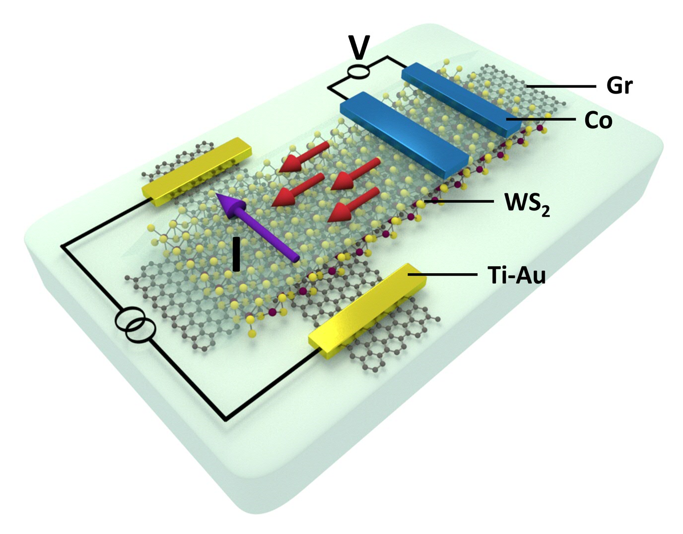
In this work, we fabricate nanodevices with single layers of graphene and WS2. We experimentally show creation of accumulation of spins and generation of spin currents only by moving electrons in the graphene channel in a specific direction. The charge current is applied by non-magnetic electrodes (made of titanium and gold) and the spin accumulation/spin current is detected by spin-sensitive ferromagnetic electrodes (made of cobalt). The efficiency of the charge-to-spin conversion mechanisms is also tunable by an electric field (applied perpendicular to the graphene plane).
The active generation of spin accumulation and spin currents only by means of pure charge currents without the need for magnetic elements in electronic circuits is of high importance for spintronic applications. This together with active control of the magnitude of spin accumulation by an electric field shows the promising role of the graphene-based van der Waals heterostructures in reaching the ultimate goal of two-dimensional spin-logic devices. The results of this experimental measurement are published in Nano Letters (T. S. Ghiasi, A. A. Kaverzin, P. J. Blah and B. j. van Wees, “Charge-to-Spin Conversion by the Rashba-Edelstein Effect in 2D van der Waals Heterostructures up to Room Temperature”, Nano. Lett. 2019,https://doi.org/10.1021/acs.nanolett.9b01611).
More news
-
-
15 September 2025
Successful visit to the UG by Rector of Institut Teknologi Bandung
-