Research
Topics and Projects
We do experimental research that focuses on the quantum physics of electron spin ensembles and nuclear spin ensembles in semiconductor devices. Current projects study electron spin manipulation and dephasing for ensembles, electron many-body effects, and quantum state transfer between spin states and optical pulses. Our work has a basis in expertise on conventional semiconductors such as GaAs, but we currently mainly explore new material systems such as color centers in wide-band-gap materials (e.g. SiC), 2D materials, and organic or hybrid organic-inorganic molecular systems. We use electron transport methods, optical pump-probe techniques and quantum optical techniques. While there is a clear link to application-driven research on quantum information technology and spintronics, our focus is on fundamental studies of quantum coherent dynamics in solid-state devices.
List of topics:
1. Quantum optics with electron spin ensembles in semiconductors
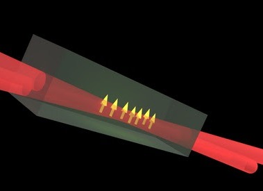
This project explores how one can map a quantum state carried by a light pulse onto a degree of freedom in solid state material, and vice versa. This may provide a new way for preparing entangled states in solid state. The approach aims at realizing an ensemble of quantum systems in a semiconductor, that have a set of energy levels similar to that of alkali atoms, and similar selection rules for the optical transitions. In these systems, long-lived quantum superpositions of low-energy states can be controlled by optical control fields (addressing high-energy transitions), by exploiting a quantum interference between two transitions that are driven at the same time (techniques based on so-called Electromagnetically Induced Transparency, EIT). At this stage, we realized EIT in GaAs and similar materials, and with the spins of color centers in SiC. This provides evidence that localized electronic spins in a semiconductor can form a medium for quantum optics. The experimental work concerns experiments that study the propagation of optical fields through optical wave guides of semiconductor material, with the quantum systems (localized donor electrons, or color-centers) inside this wave guide.
2. Spin dynamics in organic molecules and organic semiconductors
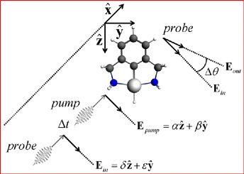
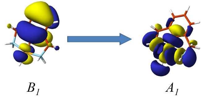
This is project a new project per 2013. The goal is to explore how the physics that underlies the spin control and optical transitions in GaAs can also occur in organic materials. Success in this direction will provide new methods for exploring the charge dynamics in organic devices, such as the organic solar cell materials that are widely studied at the Zernike Institute for Advanced Materials. We also explore how spin physics can occur in chiral/helical molecules, that we study by adhering them on graphene, and combining optical and electron-transport methods.
3. Spin-valley physics in TMDC 2D materials
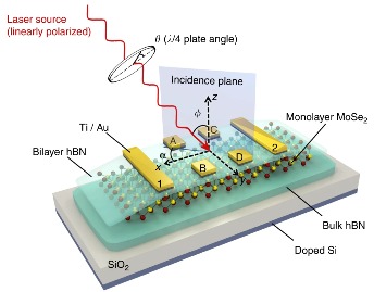
Very interesting! See this recent paper: doi – open access.
4. Optical pump-probe studies of transport and dephasing of electron spin ensembles in low-dimensional devices
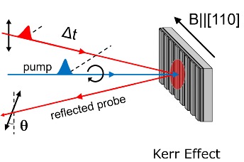
[Project not active per 2016] Time-resolved Kerr rotation measurements allow for preparing and detecting the spin states of electron ensembles in GaAs with very high (subpicosecond) time resolution. At the same time, a reasonable (around micronscale) spatial resolution can be achieved. We use this in this project to study how electron spin states evolve and dephase while they are localized or transported in diffusive micronscale devices. The electron ensembles in these devices can be low-dimensional with respect to quantum confinement, the spin precession length or the spin diffusion length. Interactions between electron spins and the environment are typically dominated by spin-orbit effects, or coupling to nuclei. We study how a lower dimensionality for an ensemble can influence spin dephasing, or can result in spin manipulation during transport. A new effort here aims at linking these techniques to spin-pumping with microwaves, and spin-injection from ferromagnets.
5. Electron many-body effects in semiconductor nanodevices
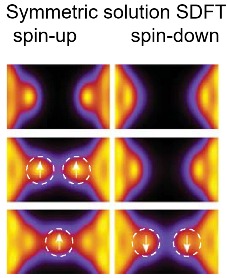
[Project not active per 2017] This project studies electron many-body effects in GaAs quantum point contacts (QPCs). These are short one-dimensional transport channels in which the electron transport is ballistic. Transport measurements on such devices reveal signatures of electron many-body effects, which include the so-called 0.7 anomaly, enhancement of the electron g-factor, and the Kondo effect. These phenomena are not yet fully understood, but very interesting and important for further developments in nano-electronics and quantum devices. By only making a narrow constriction in a clean non-magnetic semiconductor, a state is formed that shows signatures of emergent localization via the Kondo effect. We currently investigate how the constriction geometry and Coulomb effects influence the signatures of these many-body phenomena. In strong magnetic fields, electron emission from QPCs can be spin-polarized, and we also investigate how the appearance of this can be optimized.
Measurement facilities Van der Wal Labs
One setup (for visitors: building 13, room 237) has an optical table for quantum optics experiments, where the essential part is a set of two highly tunable CW Ti:Sapph lasers (M2-lasers, SolsTiS). The essential parts of the other setup (for visitors: building 13, room 144) are an optical cryostat (Oxford Spectromag, 8 T field) and a pulsed Ti:Sapph laser system (Coherent Chameleon Ultra). This room also has the new facilities for the projects with ZnSe and SiC, which are based on CW diode lasers around 443 nm, 1078 nm and 1130 nm.
Collaborations
For SiC materials, our main collaboration is the group of Nguyen T. Son and Jawad Ul-Hassan (Linköping, Sweden) . In recent years our most important collaboration for obtaining MBE grown GaAs/AlGaAs heterostructure wafer materials and high-purity n-GaAs epi-layers was with the group of Andreas Wieck in Bochum (Germany) . For MBE grown materials we will also continue to collaborate with Dirk Reuter, who started a new group in Paderborn (Germany) (after a position in Bochum till 2012).
For theory support we have various collaborations.
For nanofabrication expertise and facilities we particpate in the Dutch National Nanoned and NanoLab NL initiatives.
Funding
Our research is possible thanks to funding from the following organizations:
- The Top Research School status of the Zernike Institute of Advanced Materials
- An ERC Starting Grant (European Research Council)
- A Vidi grant (2005) and a Veni grant (2014) from the Netherlands Organization for Scientific Research (NWO)
- The Dutch Foundation for Fundamental Research on Matter (FOM)
- Participation in the Dutch NanoNed initiative.
| Last modified: | 17 September 2022 11.42 a.m. |