Piezoelectric response at the nanoscale
As predicted by Gordon E. Moore in 1965, the density of transistors on integrated circuits increases exponentially with time. In the past decades, the sizes of devices have decreased into the nanometer scale. At the same time, applications including ferroelectric or piezoelectric thin films are developing at a staggering pace. It is thus interesting to investigate the behavior of ferroelectric thin films with decreasing size, from hundreds of micrometers to tens of nanometers. At these small sizes different effects, such as the clamping of the substrate and the proximity to the critical size for the existence of cooperative action (ferroelectricity), compete and the behavior of the material becomes complex. Our goal is to answer the simple but still not totally understood questions: As the size of the device decreases, does the piezoelectric response of materials increases or decreases? and, is this trend the same for all ferroelectrics?
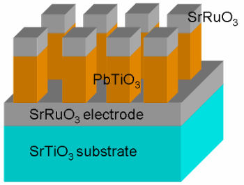
To answer these questions we deposit thin films of ferroelectric materials (PbTiO3 , BaTiO3 , etc) with thicknesss of ~50nm with top and bottom electrodes on a well matched perovskite substrate. Using UV-lithography and Electron beam Lithography (EBL), the films are shaped with lateral sizes ranging from 0.01mm to 100 nm. Polarization switching and piezoelectric behavior is studied as a function of the lateral dimensions. For the smaller sizes bellow 100nm, a technique called ferroelectric lithography is used on films with periodic nanodomains. In this way nanostructures with very small dimensions down to 5-10 nm can be achieved.