
Quantum dots form ordered material
Quantum dots are clusters of some 1,000 atoms which act as one large ‘super-atom’. It is possible to accurately design the electronic properties of these dots just by changing their size. However, to create functional devices, a large number of dots have to be combined into a new material. During this process, the properties of the dots are often lost. Now, a team led by University of Groningen professor of Photophysics and Optoelectronics, Maria Antonietta Loi, has succeeded in making a highly conductive optoelectronic metamaterial through self-organization. The metamaterial is described in the journal Advanced Materials, published on 29 October.
Quantum dots of PbSe (lead selenide) or PbS (lead sulphide) can convert shortwave infrared light into an electrical current. This is a useful property for making detectors, or a switch for telecommunications. ‘However, a single dot does not make a device. And when dots are combined, the assembly often loses the unique optical properties of individual dots, or, if they do maintain them, their capacity to transport charge carriers becomes very poor’, explains Loi. ‘This is because it is difficult to create an ordered material from the dots.’
Ordered layer
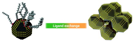
Working with colleagues from the Zernike Institute for Advanced Materials at the Faculty of Science and Engineering, University of Groningen, Loi experimented with a method that allows the production of a metamaterial from a colloidal solution of quantum dots. These dots, each about five to six nanometres in size, show a very high conductivity when assembled in an ordered array, while maintaining their optical properties.
‘We knew from the literature that dots can self-organize into a two-dimensional, ordered layer. We wanted to expand this to a 3D material’, says Loi. To achieve this, they filled small containers with a liquid that acted as a ‘mattress’ for the colloidal quantum dots. ‘By injecting a small amount onto the surface of the liquid, we created a 2D material. Then, adding a bigger volume of quantum dots turned out to produce an ordered 3D material.’
Superlattice
The dots are not submersed in the liquid, but self-orient on the surface to achieve a low energy state. ‘The dots have a truncated cubic shape, and when they are put together, they form an ordered structure in three dimensions; a superlattice, where the dots act like atoms in a crystal’, explains Loi. This superlattice that is composed by the quantum dot super atoms displays the highest electron mobility reported for quantum dot assemblies.
Detectors
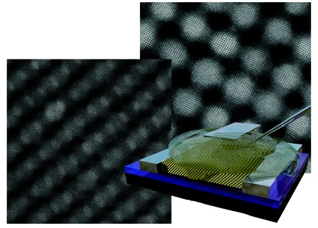
It took special equipment to ascertain what the new metamaterial looks like. The team used an electron microscope which has atomic resolution to show the details of the material. They also ‘imaged’ the large-scale structure of the material using a technique called Grazing-incidence small-angle X-ray scattering. ‘Both techniques are available at the Zernike Institute, thanks to my colleagues Bart Kooi and Giuseppe Portale, respectively, which was a great help’, says Loi.
Measurements of the electronic properties of the material show that it closely resembles that of a bulk semiconductor, but with the optical properties of the dots. Thus, the experiment paves the way to create new metamaterials based on quantum dots. The sensitivity of the dots used in the present study to infrared light could be used to create optical switches for telecommunication devices. ‘And they might also be used in infrared detectors for night-vision and autonomous driving.’
ERC Grant
Loi is extremely pleased with the results of the experiments: ‘People have been dreaming of achieving this since the 1980s. That is how long attempts have been made to assemble quantum dots into functional materials. The control of the structure and the properties we have achieved was beyond our wildest expectations.’ Loi is now working on understanding and improving the technology to build extended superlattices from quantum dots, but is also planning to do so with other building blocks, for which she was recently awarded an Advanced Grant from the European Research Council. ‘Our next step is to improve the technique in order to make the materials more perfect and fabricate photodetectors with them.’
Reference: Jacopo Pinna, K. Razieh Mehrabi, Dnyaneshwar S. Gavhane, Majid Ahmadi, Suhas Mutalik, Muhammad Zohaib, Loredana Protesescu, Bart J. Kooi, Giuseppe Portale and Maria Antonietta Loi: Approaching Bulk Mobility in PbSe Colloidal Quantum dots 3D Superlattices. Advanced Materials, 29 October 2022
| Last modified: | 01 November 2022 09.58 a.m. |
More news
-
13 May 2024
Trapping molecules
In his laboratory, physicist Steven Hoekstra is building an experimental set-up made of two parts: one that produces barium fluoride molecules, and a second part that traps the molecules and brings them to an almost complete standstill so they can...
-
29 April 2024
Tactile sensors
Every two weeks, UG Makers puts the spotlight on a researcher who has created something tangible, ranging from homemade measuring equipment for academic research to small or larger products that can change our daily lives. That is how UG...
-
16 April 2024
UG signs Barcelona Declaration on Open Research Information
In a significant stride toward advancing responsible research assessment and open science, the University of Groningen has officially signed the Barcelona Declaration on Open Research Information.